
Volume 18, Number 3, November 2015
Symmetrical Data Link For Burst Mode Transmission
- 1 Alcatel-Lucent (This work was completed while the author was with M/A COM / COBHAM).
Abstract
This paper discusses the architecture and the implementation of 5 Mbps over-the-air data rate, burst-mode data link which has the capabilities of the upstream and downstream transmission in a single module with symmetrical data rates in a time division duplex (TDD) manner. The data link operates in S band. We discuss the various RF challenges that exist on a RF system-level and show how such challenges can translate into implementable circuit designs. The reason for a TDD-based RF front end is that TDD is known to offer cost advantages as compared to FDD-based system. The additional advantage, where size is an issue, is that it uses less space compared to FDD. The fundamental subsystem blocks such as synthesizers, filters and power amplifiers are where most of the RF front end transceiver costs reside. We also discuss some of the important modem specifications for RF and baseband and the implications for the design of RF circuits, which include SNR, channel bandwidths, RF bands, noise figures, output power levels, and gain setting.
1. Introduction
With the growing need for the reduction in cost and size the challenges in designing a RF front end increases. For the radio module to operate successfully the cost versus performance equation has to be balanced carefully—that is, given the design of the RF front-end module there is a limitation on how small the board size could be without affecting modem performance. Many a time in RF design, simulation results with regards to performance often do not correlate with the experimental results, especially for small factor board designs. Therefore as a design engineer one has to know what the limits are and where the line needs to be drawn, cost versus performance. Where ever possible Radio Frequency Integrated Circuit (RFIC) integration should be used, because it enables cutting down costs through the use of integration and advanced techniques to increase link margins, should be able to achieve reliable wireless systems at a reasonable cost and form factor.
2. TDD Architecture—General Concepts
In our design we use the TDD architecture for the RF front end. TDD systems utilize one frequency band for both transmit and receive. This concept requires only one Local Oscillator (LO) for each stage of the radio. In addition only one RF filter per stage is necessary and this filter is shared between the Transmitter (TX) and the Receiver (RX). The synthesizer and RF filters are major cost drivers in radios. Having one synthesizer per stage saves on board area, a large part of the radio board size can be taken up by the LO. The RF filter in a TDD system is not required to attenuate its TX noise as severely as in FDD systems. Operation of the radio in TDD mode prevents the TX noise from self-jamming the RX since only one is on at any time. As well as relief of the RF filter specifications, having just one RF filter saves cost and space. It should be noted that to ensure transmitting radios do not interfere with nearby receiving radios, the specification for TX emission requirements cannot be eased. There is a notable savings in power from the TDD architecture, a direct result of turning the RX off while in TX mode and vice versa and as a result of this there is a reduction of data throughput since there is no transmission of data while in RX mode. It must be noted that while the RF filtering specifications are relaxed, this tends to imply that in TDD systems the transmitting radio modules will have to be spaced further apart from each other to avoid interference. The RF stage is connected to the IF block which in turn is processed by the baseband block. This structure has the advantage that some filtering is done at IF stage removing some of the strain on the dc filters. In addition, power can be saved by having the final stage operate at lower frequencies. The architecture also has the added advantage that the I/Q mismatch from the low-pass filters is removed. One drawback is that two Digital to Analogue (DA) converters are used in the receive chain.
The baseband block digitizes the analogue signal and performs signal processing. This PHY layer module contains the blocks for filtering, Automatic Gain Control (AGC), demodulation of data, security, and framing of data. The major blocks within a radio that need control from the baseband module are AGC, frequency selection, sequencing of the TX/RX chain, monitoring of TX power, and any calibration functions.
There are three main areas of cost for from the RF front-end of a radio: synthesizer, power amplifier, and filter.
Synthesizer
The synthesizer generates the LO that mixes with the incoming RF or IF signal to create a lower frequency signal that can be digitized and processed by the baseband module. Depending upon the bandwidth the specifications call for a high-performance synthesizer. The synthesizer block takes up a large part of the board area and is therefore a costly component of the RF module. It must be noted that as RF increases the phase noise also increases and obtaining a phase noise <1deg rms becomes a challenge in wideband communication systems. As well as all the radio LOs, the clock for the A/D must be also viewed as an LO that adds phase noise to the overall jitter specification.
Power Amplifier
Generally digital modulation transmitters require a high degree of linearity. The wider the bandwidth the more linear the PA’s need to be. Linearity implies higher power consumption. The trade-off between efficiency and linearity has always been a constant battle. Depending on the class of power amplifier their efficiencies can vary. Most often importance is given to the efficiency of the PA because for set output power level the power consumption of the overall modem greatly depends on it. In this process a much overlooked parameter in PA design by the designers is settling time. When a PA is switched on from cold the power level will overshoot (or undershoot), then settle out. This settling time can be as poor as 100s of millisecond to get within 0.1 dB of the final value. For certain types of modulation this is extremely important. If there is a drop of power from the beginning to the end of > 0.1dB across the frame, the BER for non-constant type modulation will increase. In cases with the droop the PA may have to be turned on ahead of the TX cycle to allow the PA to stabilize and remove some of the droop.
Filtering
Filtering is required to eliminate undesired signals from adjacent or alternate channels. Any noise from these immediate signals can leak into the desired band. Filtering at the receiver does not help, only a clean transmitted signal will prevent such degradation. For the adjacent channel problem the challenge is between linearity and filtering complexity. If the undesired channels are filtered out then less back-off in the radio is required and more of the A/D bits are available for fading margin. SAW filters have depreciated in cost and are now much cheaper than before especially if the volumes are high. SAW’s provide the optimum filtering. Filtering on the board requires a large area and as the channel bandwidth is reduced the size increases. Chip filters tend to be small but also produce more noise. For I/Q-based designs, chip filters are necessary as they can be matched much more closely, which minimizes I/Q mismatch due to filtering. The final channel selectivity is performed in the baseband module using digital filters. Filtering, like gain, must be distributed between the RF and subsequent down conversions. The RF filtering is used to reduce the image and far blockers; i.e., out of the RF band. The RF front-end must be linear enough to support the largest in-band blocker. In addition, reciprocal mixing of the LO with the undesired signal must be considered.
3. Data Link Architecture
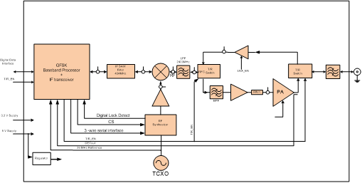
The Data Link Transceiver architecture used is designed for low data rate and low power applications. The transceiver module is mainly intended for the operation in S band. The transmit chain consists of two up conversion stages all of which are analogue while the receive chain consists of three down conversion stages, the first two stages being analogue while the final stage being digital as shown in Figure 1.
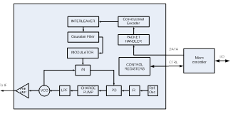
A simplified block diagram of the Data Link transmitter and receiver is shown in Figures 2 and 3 respectively. The transceiver configuration can be optimized to achieve the best performance for the upstream / downstream data link application. Through the control registers the following key parameters can be programmed:
- RF output power
- RF output frequency
- GFSK frequency separation (deviation)
- Crystal oscillator reference frequency
- Power-down / power-up mode
- Data rate
- UART interface
- DMA buffers
- SPI interface
- Synthesizer lock indicator mode
- RSSI output
3.1 Transmitter
The data received from the computer via the baseband processor interface is buffered using the DMA channels. This data is then processed by the packet handler. Here the preamble depending on the programmable number of bytes is added. A 4 byte sync word and the CRC (16 bits) computed over the data field is added. The data along with the CRC checksum is taken and whitened using a PN sequence which is then encoded using convolutional ½ rate code and then interleaved. This binary bit stream is then pulse shaped using a Gaussian pulse shaping filter. The pulse shaped output is then modulated (GFSK) and sent to the divide by N block of the synthesizer. The frequency synthesizer consists of a reference oscillator, phase detector (PD), CHARGE PUMP, internal loop filter which is a low pass filter (LPF), voltage control oscillator (VCO) and the frequency dividers (/R and /N) as shown in Figure 2.
The output of the VCO is fed to the pre amplifier (PRE AMP) and the output at the IF stage is Gaussian Frequency Shift Keyed (GFSK). The output of the first IF stage is then filtered through an IF SAW filter and up converted to the S-band via the RF mixer. The output of the mixer with the signal now at RF is filtered once again using a LPF as shown in figure 1. This output is filtered by means of a band-pass filter before it is amplified by the power amplifier (PA). The output of the PA is again filtered by another band-pass filter before it is propagated out through the antenna as shown in Figure 1.
The data to be transmitted is stored in the RF transmit buffer which is 16-bit register in the form of 16 bit word of data. The buffering scheme shifts out bits of 16-bit shift register to the modulator one at a time, MSB first, at periods specified by the selected baud rate. When this shift register is empty it will load new data word from buffer register and continue shifting out bits. The contents of the buffer register remain unchanged after a shift register load. An interrupt request is generated once the contents of the shift register are transmitted so that the shift register can be loaded with a new data word. If a new word is not written within 16 bit periods (sixteen baud periods in NRZ mode) the shift register will continue to load the same data in the buffer register.
Data transmission is started once the word of information is placed in the transmission buffer and the transmit chain is enabled. This assumes that the all the components in the transmit chain are properly calibrated and the synthesizers and the VCO are in lock. It is especially important to take the buffering scheme into account at the end of a transmission. When the last byte of a data frame or packet is loaded into the shift register it is still not transmitted. Thus the interrupt request generated at the same time must not turn off either analogue or digital parts of the transmit chain. The transmission cannot be ended safely until a certain period of time when the last bit has been shifted out and has propagated through the transmit chain to the antenna. A simple solution is to transmit a couple of dummy bytes at the end of the real data content.
3.2 Receiver
The receiver consists of two stage conversion process. The received GMSK signal in the C band is suitably filtered and amplified using a low noise amplifier (LNA1) after which it is down converted to the first IF stage as shown in Figure 1. This IF signal is further amplified by the low noise amplifier (LNA2) and down-converted in quadrature (I and Q) to the intermediate low frequency (IF) which is the second IF stage. At low IF, the I/Q signals are digitized by the analogue to digital converters (ADCs) as shown in Figure 3. Automatic gain control (AGC), fine channel filtering, demodulation which will bring the signal to baseband and bit/packet synchronization are performed digitally. The GMSK demodulator is in the digital domain which after demodulating the received signal to baseband is sent for further processing by the channel filter and frequency offset compensator. The frequency offset compensator compensates for the offset that is introduced between the transmitter and the receiver within certain limits by first estimating the offset and then is automatically adjusted for the offset by means of synthesizer. The received signal strength indicator (RSSI) is generated by estimating the signal strength in the channel. The signal is then processed by the data filter the output of which will be symbols. Since the modulation is GFSK each of the symbols is a bit.
The data in the bit format is synchronized by extracting the clock from the incoming data bits (symbols). For the synchronization process to work it is assumed that the registers of the transmitter and the receiver are suitably configured such that the data rates are fixed. Re-synchronization is performed continuously such that the error in the incoming symbol rate is adjusted.
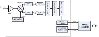
Once the data in the bit form is obtained byte synchronization is carried out using a 16 bit sync word which is repeated to get a 32 bit sync sequence. The demodulator uses this field to find the word boundaries in the stream of bits. This sync word acts as a system identifier since only the predefined packets with the correct sync word will be received by the receiver. A preamble sequence is used prior to the sync word which needs to be detected as well.
The receiver after demodulation performs:
- Preamble detection
- Sync detection
- Packet length check
- Address check
- CRC check
- De-whitening of the received data
- De-interleaving
- FEC decoding
Data whitening is done using a pseudo random sequence before being transmitted and the same pseudo random sequence is used to de-whiten the received data. Forward error correction in the form of ½ rate convolutional coding with a constraint length of 4 is employed on the data field and CRC word in order to reduce the bit error rate when operating near the sensitivity limit. So it can viewed that for a given SNR, FEC decreases the bit-error rate (BER) thus extending the range. The need for FEC is that in radio environments transients and interference will produce errors, even in otherwise good reception conditions. FEC will mask such errors and combined with interleaving of coded data will be able to correct even relatively long periods of faulty reception. The use of FEC however will require a higher receiver bandwidth and therefore the overall coding gain should be calculated by combining the two factors the coding gain due to the code plus the degraded sensitivity due to the increase in receiver bandwidth. Interleaving following coding is used to correct for burst errors arising due to channel interference. A block inter-leaver is used for this purpose. When FEC and interleaving is used at least one extra byte is required for trellis termination. For this reason 4 extra bytes are used in our modem.
The RF transmit power is 36 dBm (4 W), and the receiver sensitivity which depends not only on the data rate but also on FSK separation is targeted at –96 dBm. The operating frequency band is S band (2200 MHz – 2900 MHz).
4. Data Link Implementation
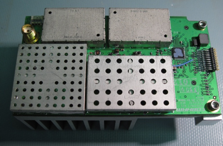
The data link transceiver module is as shown in Figure 4. The modules are designed and assembled using off the shelf components based on the architecture and the functionality discussed in Section 3. The key features for the transmitter and receiver implementation are in Table 1 and 2.
5. Data Link—PC Interface
The setup for transmission is shown in Figure 5. The radio transmission setup consists of a PC connected to the data link one of which is configured to operate in the transmit mode. In the case of transmission when data is to be transmitted a graphical user interface (GUI) is invoked at the PC.
For the demonstration of the working of the data link information which is entered using the PC terminal is transmitted by means of the serial interface which is interrupt driven to the wireless data link module using the DMA channel.
Similarly on the receiver side the received data is sent to the PC terminal. The data is sent to the PC by calling the required interrupt service routine needed for the communication interface. For test purposes a transmit terminal and receive terminal GUI for transmit and receive terminal sides is used.
The above setup assumes that there are 2 PCs, one which connects to the transmit RF module and the other connects to the receive RF module. The program within is set to the appropriate parameters, which makes it easier for the user to use it for test purposes.
| Parameter | Value | Comments |
|---|---|---|
| Frequency Range | 2200 – 2290 MHz | Up or Downlink Transmit |
| Operation | Half Duplex | |
| Modulation | GFSK | |
| Raw Bit Rate | 5 Mbps | |
| Max output power | 36 dBm (typical) | With a 5 Mbps bit rate. |
| Interface | Parallel interface | |
| Applicable Standards | IRIG-106 and Mil-Std 461 D |
| Parameter | Value | Comments |
|---|---|---|
| Frequency Range | 2200 – 2290 MHz | Up or Downlink Receive |
| Operation | Half Duplex | |
| Modulation | FSK, NRZ-L | |
| Raw Bit Rate | 5 Mbps | |
| Data payload | 100 bytes | fixed |
| Sensitivity | –96 dBm | Typical for 5 Mbps |
| IF Bandwidth | 10 MHz | With a 5 MHz bit rate. |
6. Results
The modem was tested to check its performance over the operating frequency band (2200 MHz – 2290 MHz) at a output transmit power of 36 dBm. With the Receiver at –96 dBm the data link was found to be successfully operating in the burst mode with a packet size of 100 data bytes. The total packet size for the transmission of 100 bytes of data is 125 bytes without error correction.
7. Conclusions
The system has been successfully tested for operation over the air for the data and formats specified. Performance of the data link with regards to mobility and distance needs to be checked. From the tests performed in the lab it is observed that in order to achieve the desired sensitivity it is very important that the modules are properly shielded and leakage is prevented.
References
[1] Telemetry Standards, IRIG Standard 106-04, Part 1.